
Key Applications of Injection Molding in Consumer Electronics
The versatility of the injection molding process has made it indispensable across virtually all categories of consumer electronics and communication devices. Understanding these applications provides insight into why this manufacturing method continues to dominate the industry.
Smartphone and Tablet Casings
Modern smartphones and tablets rely heavily on injection-molded components for their outer housings and internal structural elements. Manufacturers carefully select polymers that balance durability, weight, and aesthetic appeal.

High-performance polycarbonate (PC) and acrylonitrile butadiene styrene (ABS) blends are commonly used for their excellent impact resistance and dimensional stability. These materials can withstand daily wear while maintaining the device’s sleek appearance. For premium devices, manufacturers often incorporate glass-filled nylon or liquid crystal polymers (LCP) to enhance structural integrity without adding significant weight.
The injection molding process allows for precise control over surface textures and finishes, enabling manufacturers to create devices with both visual appeal and ergonomic grip. Advanced techniques like in-mold decoration (IMD) and in-mold labeling (IML) integrate graphics and textures directly during the molding process, eliminating secondary operations and improving durability.
For waterproof devices, manufacturers employ specialized two-shot or overmolding techniques to create seamless seals between components. This approach allows for the integration of rigid structural elements with flexible gaskets in a single manufacturing step, significantly improving production efficiency while enhancing product performance.
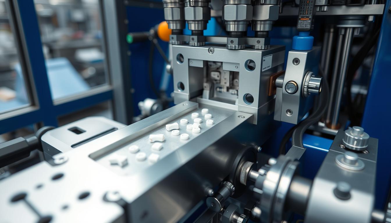
Precision Connectors and Ports
The reliability of modern electronic devices depends significantly on the quality of their connection interfaces. USB-C, HDMI, and other ports require exceptional dimensional accuracy to ensure proper connectivity and longevity.
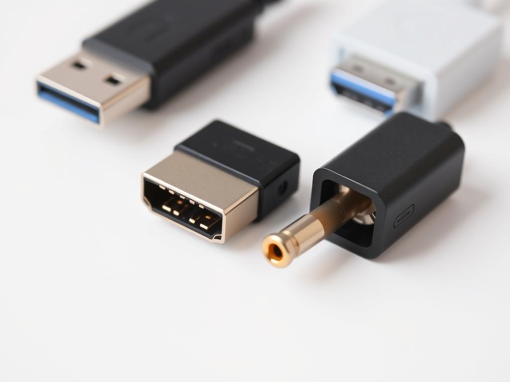
Injection molding enables the production of these critical components with tolerances as tight as ±0.05mm. This precision is achieved through careful mold design, advanced process control, and specialized high-flow engineering polymers like polybutylene terephthalate (PBT) and liquid crystal polymers (LCP).
These materials offer excellent dimensional stability, electrical insulation properties, and resistance to the heat generated during soldering operations. Additionally, they can be formulated with flame-retardant additives to meet stringent safety standards required for consumer electronics.
Heat-Resistant Components for Network Equipment
Routers, modems, and other networking equipment operate continuously, generating significant heat that must be managed effectively. Injection-molded components play a crucial role in both the structural housing and thermal management systems of these devices.
High-temperature thermoplastics like polyphenylene sulfide (PPS) and polyetherimide (PEI) are commonly used for components that must maintain dimensional stability and mechanical properties at elevated temperatures. These materials can withstand continuous operating temperatures of 150°C or higher without degradation.
The design flexibility offered by injection molding allows for the integration of complex internal structures that enhance airflow and heat dissipation. Manufacturers can incorporate features like heat sink mounting points, ventilation channels, and fan housings directly into the molded components, optimizing thermal performance while minimizing assembly complexity.

Miniaturized Parts for Wearable Technology
The explosive growth of wearable technology has pushed injection molding capabilities to new limits of miniaturization. Devices like wireless earbuds, smartwatches, and fitness trackers require incredibly small yet precise components.

Micro-injection molding techniques can produce parts weighing less than 0.1 grams with features as small as 0.05mm. These capabilities are essential for creating the housings for wireless earbuds, internal components for smartwatches, and structural elements for other wearable devices.
Materials for these applications must balance multiple requirements, including biocompatibility for skin contact, durability for daily use, and aesthetic appeal. Thermoplastic elastomers (TPE) are frequently used for components that contact the skin, providing comfort while maintaining structural integrity.
Material Innovations Driving Electronics Manufacturing
The evolution of consumer electronics has been closely tied to advancements in polymer science. Today’s injection molding materials offer unprecedented combinations of properties that enable the latest generation of electronic devices.
High-Performance Engineering Plastics

Polybutylene terephthalate (PBT) has become a staple in electronics manufacturing due to its excellent electrical properties, dimensional stability, and resistance to heat and chemicals. Its low moisture absorption makes it ideal for components that must maintain precise dimensions in varying environmental conditions.
Liquid crystal polymers (LCP) represent the cutting edge of materials technology for miniaturized electronic components. These materials offer exceptional flow characteristics that enable the molding of ultra-thin walls (down to 0.2mm) with complex geometries. Their inherent flame retardancy, chemical resistance, and dimensional stability make them perfect for mission-critical components in high-end devices.
EMI-Shielding Compounds
As electronic devices pack more functionality into smaller spaces, electromagnetic interference (EMI) has become a significant design challenge. Specialized injection molding materials now incorporate conductive fillers to provide integrated EMI shielding.
Carbon-filled compounds utilize carbon fiber or carbon nanotubes to create a conductive network within the polymer matrix. These materials can achieve shielding effectiveness of 30-40 dB across a wide frequency range while maintaining good mechanical properties and processability.
Metal-filled polymers incorporate microscopic metal particles (typically aluminum, copper, or nickel) to provide enhanced shielding performance up to 60-70 dB. Recent innovations have focused on optimizing particle size and distribution to improve flow characteristics during molding while maintaining shielding effectiveness.
Sustainable and Biodegradable Alternatives
The electronics industry is increasingly prioritizing sustainability, driving innovation in eco-friendly injection molding materials. These new formulations aim to reduce environmental impact without compromising performance.
Bio-based polymers derived from renewable resources like cornstarch or sugarcane are gaining traction for non-critical components. Materials like polylactic acid (PLA) and polyhydroxyalkanoates (PHA) offer biodegradability while providing adequate mechanical properties for applications like accessory housings and packaging.
Recycled content polymers blend post-consumer or post-industrial plastic waste with virgin material to reduce environmental footprint. Advanced sorting and processing technologies have enabled the production of recycled compounds that meet the stringent quality requirements of consumer electronics.
Design Considerations for Electronic Components
Successful injection molding for consumer electronics requires careful attention to design details that impact both manufacturability and product performance. Engineers must balance aesthetic requirements with functional needs while ensuring efficient production.
Overmolding for Waterproofing and Protection
Overmolding has revolutionized the production of water-resistant and waterproof electronic devices. This multi-step injection process creates seamless bonds between different materials, enabling enhanced protection and functionality.
In a typical application, a rigid structural component is molded first, followed by a second shot of thermoplastic elastomer (TPE) that forms gaskets, seals, or protective layers. The chemical bond between the two materials creates a waterproof barrier without requiring additional assembly steps or adhesives.
Design considerations for effective overmolding include material compatibility, appropriate undercuts for mechanical interlocking, and gate placement to ensure complete filling of the second material without disturbing the first component. When properly executed, this technique can achieve IP67 or higher waterproof ratings for consumer devices.
Tolerance Requirements for 5G and mmWave Devices
The rollout of 5G technology has introduced unprecedented precision requirements for injection-molded components. Millimeter wave (mmWave) frequencies are particularly sensitive to dimensional variations that can impact signal integrity.

Antenna housings and waveguides for 5G devices typically require tolerances of ±0.025mm or tighter to maintain proper signal characteristics. Achieving these tolerances demands precise mold design, tight process control, and materials with minimal shrinkage and warpage.
Advanced simulation tools like Moldflow analysis have become essential for predicting and compensating for material behavior during molding. These simulations help engineers optimize gate locations, cooling channel design, and process parameters to achieve the required dimensional accuracy consistently.
Design for Assembly and Serviceability
Modern electronic devices must balance sleek, integrated designs with practical considerations for assembly and potential repair. Injection molding offers unique opportunities to address these sometimes conflicting requirements.

Snap-fit features can be directly incorporated into molded components, eliminating the need for screws or other fasteners. When properly designed, these features allow for secure assembly while still enabling disassembly for repairs or component upgrades. The key is balancing the mechanical properties of the chosen polymer with the geometry of the snap features.
Internal mounting features like bosses, standoffs, and alignment pins can be integrated directly into housing components, simplifying assembly and improving accuracy. These features must be designed with proper draft angles and wall thickness transitions to avoid molding defects like sink marks or voids.
Case Study: Injection Molding in Flagship Smartphone Production
A leading smartphone manufacturer recently revolutionized their production process by implementing advanced injection molding techniques for their flagship device. This case study examines how strategic material selection and process innovations addressed key challenges in modern electronics manufacturing.

Challenge: Balancing Thinness with Durability
The design team aimed to create the thinnest device in the company’s history while improving drop resistance—seemingly contradictory goals. The housing needed to maintain structural integrity despite having walls as thin as 0.8mm in some areas.
Solution: Multi-Material Approach
Engineers developed a hybrid structure using a glass-fiber reinforced polycarbonate frame overmolded with a specialized impact-absorbing thermoplastic elastomer at strategic locations. This approach concentrated reinforcement where structural rigidity was needed while adding energy-absorbing materials at impact-prone areas.
The manufacturing team implemented advanced process monitoring with in-mold sensors to control cavity pressure and temperature throughout the injection cycle. This real-time data allowed for dynamic adjustments to ensure consistent part quality despite the challenging thin-wall design.

Results: Performance Improvements
The resulting device achieved a 15% reduction in thickness compared to the previous generation while improving drop test performance by 30%. The integrated production approach reduced assembly time by eliminating multiple components and fasteners, leading to a 22% decrease in manufacturing costs.
This case demonstrates how advanced injection molding techniques can resolve seemingly contradictory design requirements in modern consumer electronics, delivering improvements in both performance and manufacturing efficiency.
Challenges and Solutions in Electronics Injection Molding
Despite its many advantages, injection molding for consumer electronics presents several technical challenges that manufacturers must overcome to produce high-quality components consistently.
Warping in Thin-Walled Designs
Thin-walled components are particularly susceptible to warping due to uneven cooling and internal stresses. This issue is especially problematic for electronic housings where dimensional accuracy affects both aesthetics and functionality.
Advanced mold temperature control systems like variotherm technology actively manage mold surface temperature throughout the injection cycle. By rapidly heating the mold before injection and cooling it after filling, these systems reduce internal stresses and minimize warpage.
Material selection also plays a crucial role in managing warpage. Glass-filled compounds improve dimensional stability but require careful gate placement and flow path design to prevent fiber orientation issues that can cause uneven shrinkage.
Maintaining Conductivity in Antenna-Integrated Components
Modern devices increasingly integrate antennas directly into structural components, creating unique manufacturing challenges. These components must maintain precise electrical properties while meeting structural requirements.

Laser Direct Structuring (LDS) has emerged as a leading solution for creating conductive paths on injection-molded parts. This process uses specially formulated polymers containing metal-organic additives that can be activated by laser energy. After molding, a laser traces the antenna pattern, activating the additives, and subsequent metallization creates the conductive pathway.
Two-shot molding offers an alternative approach, combining a structural polymer with a second conductive polymer in a single part. This technique requires precise control of material compatibility and processing parameters to ensure proper adhesion between the two materials while maintaining the required electrical properties.
Surface Finish and Cosmetic Requirements
Consumer electronics demand flawless surface finishes that combine aesthetic appeal with functional requirements like scratch resistance and tactile feel.
In-mold decoration (IMD) and in-mold labeling (IML) techniques apply graphics or textures directly during the molding process. These approaches eliminate secondary operations while providing superior durability compared to post-mold decoration.
Physical vapor deposition (PVD) coating applied to molded parts creates metallic finishes with exceptional scratch resistance. When combined with selective masking, this technique can create striking visual effects while maintaining radio frequency transparency in areas covering antennas.

Future Trends in Consumer Electronics Injection Molding
The intersection of injection molding technology and consumer electronics continues to evolve rapidly, with several emerging trends poised to reshape the industry.
Micro-Injection Molding for IoT Devices
The explosive growth of Internet of Things (IoT) devices is driving demand for increasingly miniaturized components with complex geometries. Micro-injection molding is evolving to meet these challenges.
 Advanced micro-molding systems can now produce parts with features as small as 10 microns and weights below 0.001 grams. These capabilities enable the production of miniature sensors, connectors, and structural components for next-generation IoT devices.
New tooling approaches using additive manufacturing to create mold inserts with micro-features are reducing lead times and costs for these specialized components. This hybrid manufacturing approach combines the precision of traditional machining with the geometric freedom of 3D printing.
AI-Driven Quality Control Systems

Artificial intelligence is transforming quality control in injection molding facilities. Machine learning algorithms can detect subtle defects that might escape traditional vision systems, significantly improving yield rates for high-precision electronic components.
Predictive maintenance systems use AI to analyze process data and predict potential failures before they occur. By monitoring parameters like injection pressure, temperature profiles, and cycle times, these systems can detect deviations that might indicate developing issues with the mold or machine.
Integration with Additive Manufacturing
The boundaries between injection molding and additive manufacturing are blurring, creating new opportunities for hybrid production approaches that leverage the strengths of each technology.
Conformal cooling channels created through additive manufacturing can dramatically improve mold performance for complex electronic components. These optimized cooling systems follow the contours of the part, providing more uniform temperature control and reducing cycle times by up to 40%.
Multi-material components that combine injection-molded structural elements with 3D-printed functional features represent an emerging frontier. This approach enables the creation of complex geometries with embedded electronics, sensors, or specialized materials that would be impossible to produce with either technology alone.
Sustainability in Electronics Injection Molding
Environmental considerations are becoming increasingly important in consumer electronics manufacturing, driving innovations in materials and processes that reduce environmental impact while maintaining performance.
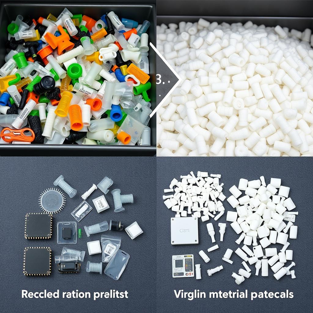
Recycled Material Usage
The electronics industry is making significant strides in incorporating recycled materials into injection-molded components without compromising quality or performance.
Post-consumer recycled (PCR) plastics are being successfully incorporated into non-critical components like accessory housings and packaging. Advanced sorting and cleaning technologies have improved the consistency and properties of these materials, making them viable for more applications.
Closed-loop recycling programs collect and process end-of-life electronic devices, recovering plastics for reuse in new products. These programs reduce waste while providing a reliable source of high-quality recycled materials with known composition and properties.
Energy-Efficient Molding Processes
Energy consumption represents both a significant cost and environmental impact in injection molding operations. New technologies are reducing this footprint while improving productivity.
 All-electric injection molding machines have replaced hydraulic systems in many electronics manufacturing facilities, reducing energy consumption by up to 70%. These machines offer precise control while eliminating the energy losses associated with hydraulic systems.
Heat recovery systems capture waste heat from the molding process and redirect it for facility heating or preheating material. This approach can reduce overall energy consumption by 15-30% while improving process stability through more consistent material temperature.
Design for Disassembly and Recycling
Forward-thinking manufacturers are designing electronic products with end-of-life considerations in mind, making disassembly and material recovery more feasible.

Compatible polymer selection ensures that different plastic components can be recycled together without contamination. This approach simplifies the recycling process while improving the quality and value of the recovered materials.
Modular design approaches allow for easier separation of components at end-of-life, facilitating both repair and eventual recycling. These designs often use snap-fit assemblies instead of adhesives or multi-material components that would be difficult to separate.
Frequently Asked Questions
Why is injection molding preferred over 3D printing for consumer electronics?
Injection molding offers several advantages over 3D printing for high-volume electronics production. The process provides superior surface finish, consistent mechanical properties, and significantly faster production rates once tooling is established. While 3D printing excels at prototyping and low-volume production, injection molding can produce thousands of identical parts per hour at a fraction of the per-unit cost, making it ideal for consumer electronics manufacturing.
What are the most important material properties for injection-molded electronic components?
Key material properties include dimensional stability (to maintain precise tolerances), heat resistance (for soldering and operating conditions), flame retardancy (to meet safety standards), electrical insulation properties, and impact resistance. For specific applications, additional properties like chemical resistance, UV stability, or EMI shielding capabilities may be critical. Material selection must balance these technical requirements with processability and cost considerations.
How does injection molding support the miniaturization trend in electronics?
Advanced injection molding techniques enable the production of increasingly miniaturized components through innovations like micro-molding (for tiny parts with microscopic features), thin-wall molding (for lightweight, space-efficient housings), and multi-material molding (for integrating multiple functions in a single component). These capabilities, combined with high-flow polymers and precise process control, allow manufacturers to create the intricate, compact components essential for modern wearables, smartphones, and IoT devices.
What sustainability improvements are being made in electronics injection molding?
The industry is advancing sustainability through several approaches: incorporating recycled and bio-based materials, implementing energy-efficient all-electric molding machines, designing products for easier disassembly and recycling, reducing material usage through simulation-optimized designs, and developing closed-loop manufacturing systems that recapture and reuse production scrap. These initiatives reduce environmental impact while often delivering cost savings and performance improvements.
Conclusion
Injection molding continues to be the backbone of consumer electronics manufacturing, enabling the production of increasingly complex, miniaturized, and feature-rich devices. As we’ve explored, the process offers unparalleled advantages in terms of precision, scalability, and cost-effectiveness for high-volume production.
The ongoing evolution of materials, design approaches, and manufacturing technologies is expanding the capabilities of injection molding to meet the ever-more-demanding requirements of modern electronic devices. From smartphones and wearables to networking equipment and IoT sensors, injection molding in consumer electronics and communications will remain a critical manufacturing process driving innovation in the industry.
As sustainability concerns grow in importance, the injection molding industry is responding with more environmentally friendly materials and processes that reduce waste and energy consumption without compromising performance. These developments ensure that injection molding will continue to shape the future of consumer electronics manufacturing in an increasingly connected world.
Need Precision Components for Your Electronics Project?
Our engineering team specializes in high-precision injection molding for consumer electronics and communication devices. Get expert advice on material selection, design optimization, and manufacturing processes.
Ready to Optimize Your Electronics Manufacturing?
Our team of injection molding specialists can help you navigate material selection, design optimization, and production scaling for your consumer electronics projects.